C35B4O1

Main Features
- Mature opto CMOS technology
- Derived from C35B4C3 technology
- Integration of photodiodes near digital/analog electronics
Technology Characteristics
- 0.35µm technology node
- 200mm wafer size
- 19 masks
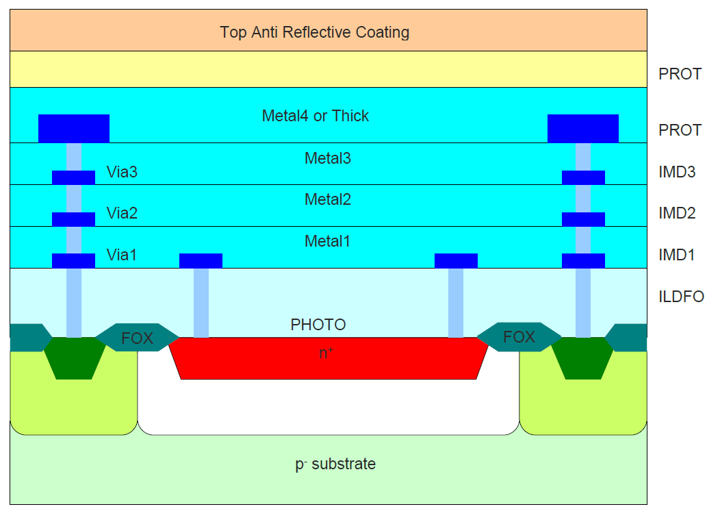
- Epitaxial growth of p-epi layer on p-type substrate to lower the photodiode dark current
- LOCOS isolation
- 3.3V and 5V operating voltages
- 4 metal (AlCu) layers for interconnexion
- Deposition of anti-reflective coating on passivation layer to increase light transmission through the back-end stack
- Second poly layer for resistors and capacitors
- Poly-insulator-poly capacitor (0.9fF/µm²)
- 1 GHz max operating frequency
- Qualified from -40°C to 125°C, for automotive and medical markets
RAM, EEPROM and OTP memories (poly fuses) available on request
Wafer cross section of the photodiode (Arc process option)
Prices
- 800 euros/mm²
- 700 euros/mm² for registered Europractice member
- Minimum billing area of 20 mm²
- Delivery of 40 bare dies
Contact
Design-Kit Content
Basic libraries:
- Primitive devices
- Primitive RF devices
- Primitive ESD devices
Analog libraries:
- Low-voltage analog standard cells
- 4 metal analog power supply pads & analog I/O pads
- 4 metal 3-bus analog power supply pads & analog I/O pads
- Core-limited 4 metal 3-bus analog power supply pads & analog I/O pads
Digital libraries:
- 3.3V digital standard core cells
- Dense 3.3V digital standard core cells
- 5V digital standard core cells
- 3-bus 3.3V digital standard cells
- Dense 3-bus 3.3V digital standard cells
- 3-bus 5V digital standard core cells
- 4 metal digital input/output/bidirectional buffers & power pads – 3.3V supply
- 4 metal digital input/output/bidirectional buffers & power pads – 5V supply
- 4 Metal 3-Bus digital input/output/bidirectional buffers & power pads – 3.3V supply
- Core-limited 4 metal 3-bus digital input/output/bidirectional buffers & power pads – 3.3V supply
- Core-limited 4 metal digital input/output/bidirectional buffers & power pads – 5V supply
CAD Tools
Cadence
- Virtuoso ADE suite (design exploration and analysis)
- Genus (physical synthesis)
- Spectre (electrical simulation)
- Xcelium (logic simulation)
- Assura (physical verification)
- Quantus (parasitic extraction)
- Voltus (power analysis)
- Innovus (digital implementation)
Siemens
- Calibre (physical verification)
- QuestaSim (logic simulation)
- QuestaFormal (formal verification)
Synopsys
- VTRAN (design exploration and analysis)
- Design compiler (physical synthesis)
- PrimeTime (static timing analysis)
- HSpice (electrical simulation)
Run Dates
- 3 MPW runs per year
- Usually in February, July and November
- Next submission deadline to CIME-P: please refer to the run schedule.
Turnaround Time
- 12 weeks from foundry tape-out to wafer fab-out
- 5 additional weeks for dicing and packaging

