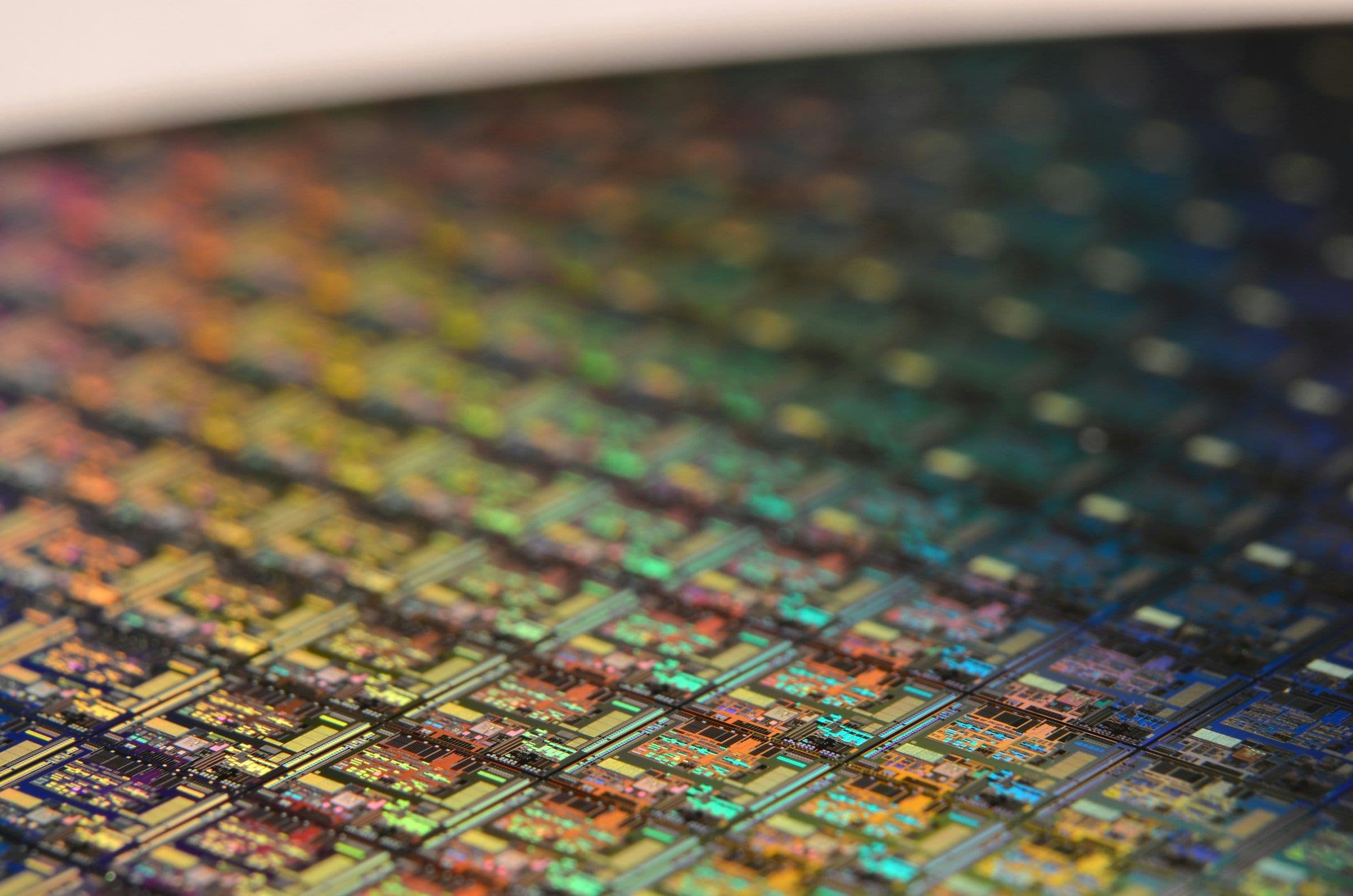
Multi-Project Wafer service
From idea to silicon.
Direct access to the world’s leading semiconductor foundries, with the cost shared across a single wafer.
A semiconductor foundry, within reach.
Industrial-grade.
Tape out on the very processes used in production by Europe's leading foundries, no toy nodes, no compromises.
Shared, not steep.
A Multi-Project Wafer run splits one mask set across many designs. You pay for the millimetres you use, not a whole wafer.
Open to all.
No selection committee and no competition for slots, clear a simple technical check and you're on the next run.
Four steps to first silicon.
Design
Lay out your circuit against the real process design kits (PDKs) of our partner foundries.
Submit
Upload your design through our dedicated CRM and reserve your place in the next run.
Fabricate
Your design joins a shared wafer and runs on a qualified industrial production line.
Validate
Get your chips back, and characterise them on-site, electrically and in RF up to 220 GHz.
One platform. Every technology.
Whatever you’re building, there’s a process for it.


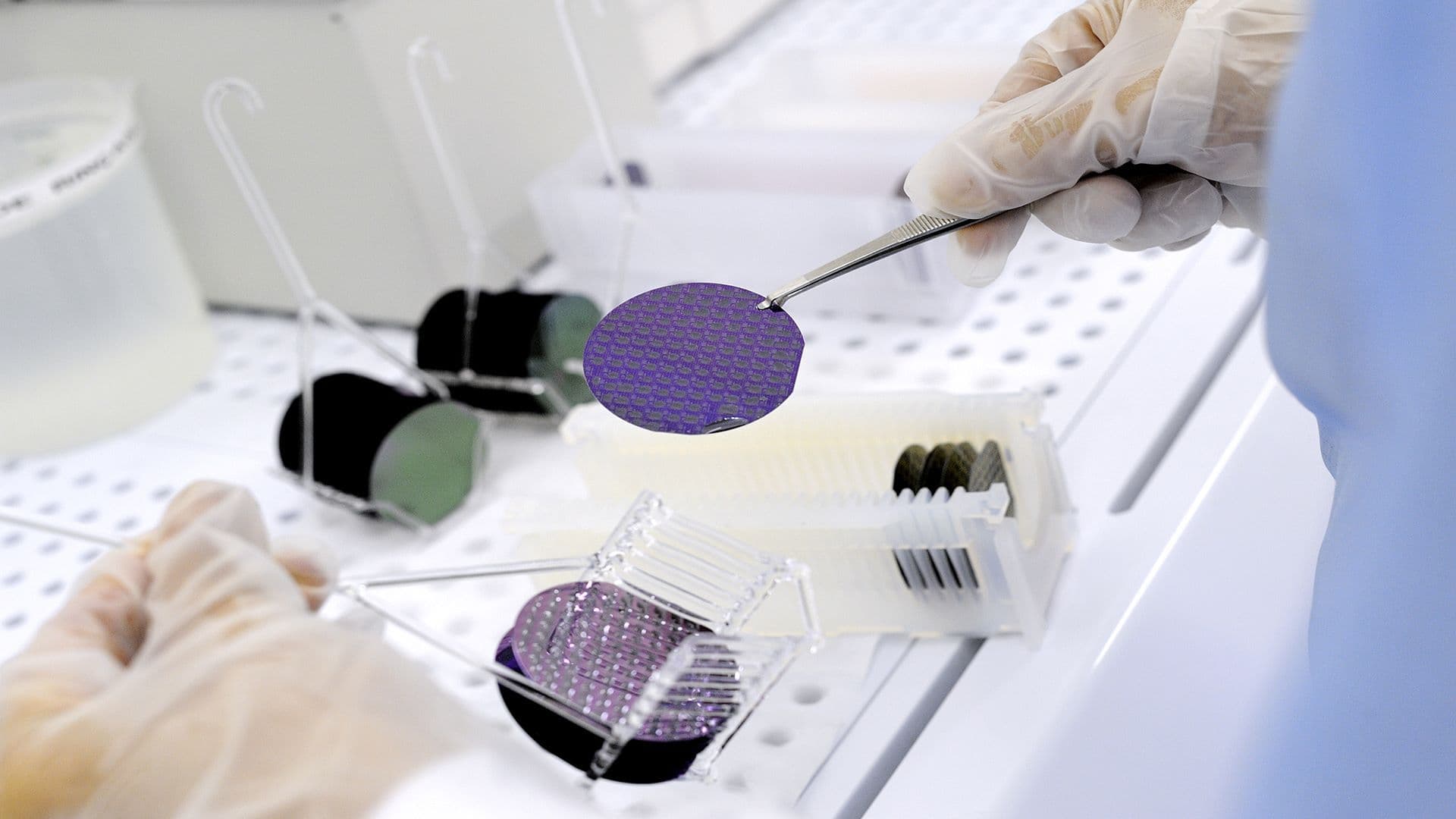
Direct access to world-leading foundries




The Multi-Project Wafer model.
Why buy a whole wafer when you only need a few square millimetres?
A full mask set can cost hundreds of thousands of euros. By placing many independent designs side by side on a single wafer, CIME-P shares that cost across every project on the run, the same industrial quality, at a price research budgets can actually meet.
Built for whoever’s building.
Academics & labs
Turn research ideas into measured silicon, on the same processes as industry.
Startups
De-risk your first chip without committing to a full mask-set budget.
Industry
Prototype and qualify new designs alongside trusted foundry processes.
Education
Give students hands-on access to genuine semiconductor fabrication.
Ready to fabricate?
Reserve your slot in the upcoming Multi-Project Wafer run, or submit your design through our CRM.